PCB Assembly Equipment
**BERGEN Group** offers process and equipment for Surface Mount Technology(SMT) , Plated Through Hole Technology(PTH) production lines from our various European Partners. In addition we offer allied tools and instruments for Research and Development(R&D), SMT rework and handling, 3D automatic optical inspection system (AOI), 3D solder paste inspection equipment & 3D x-ray inspection system.
Applications
19 applications
3D Solder Paste Inspection
### Enhance Your PCB Assembly Process with Advanced 3D Solder Paste Inspection (SPI) Our cutting-edge 3D Solder Paste Inspection (SPI) machines are designed to identify and rectify defects at the root cause, ensuring the highest quality in your PCB assembly process. With more than 60% of PCB defects originating in the front-end of the assembly process, our SPI systems offer a vital solution to optimize your production line and reduce errors. #### Key Features: **3D SPI Technology:** Utilize the latest 3D Solder Paste Inspection technology to accurately detect and measure solder paste deposits, ensuring precise and reliable results. **Laser Line Scan & Optical Methods:** Choose between laser line scan and optical inspection methods, offering versatility and accuracy tailored to your specific needs. **Industry-Leading Inspection Speed:** Benefit from the fastest inspection speed in the industry, minimizing downtime and maximizing production efficiency. **Real 3D Imaging:** Gain unparalleled insight with real 3D imaging that provides detailed visualization of solder paste applications, enhancing defect detection capabilities. **Color and Material Irrelevant Inspection:** Perform inspections that are unaffected by variations in color, material, or surface roughness, ensuring consistent and reliable results across different PCB types. **Automated PCB Warpage Measurement:** Automatically measure PCB warpage, allowing for precise adjustments and ensuring optimal alignment during the assembly process. **Automated PCB Stretch and Shrinkage Compensation:** Automatically compensate for PCB stretch and shrinkage, maintaining accuracy and consistency in your production line. **Process Optimization with Feedback & Feedforward Linkage:** Optimize your assembly process with feedback and feedforward linkage support, allowing for real-time adjustments and improved overall performance. **Comprehensive Inspection Capabilities:** Inspect a wide range of parameters including height, area, volume, offset, bridging, shape, PCB warpage, and PCB shrinkage, ensuring thorough quality control at every stage. ###### Our 3D SPI machines are engineered to enhance the quality and efficiency of your PCB assembly process, helping you to minimize defects and optimize production. Trust our state-of-the-art inspection technology to deliver the accuracy and reliability you need to stay ahead in the competitive electronics manufacturing industry.
Automatic Optical Inspection System
### Enhance Production Efficiency with Our PCB Automatic Optical Inspection (AOI) System Our cutting-edge PCB Automatic Optical Inspection (AOI) system is designed to cater to various sizes of PCB assemblies, significantly boosting production efficiency and reducing costs across electronic manufacturing services, the communication industry, and beyond. 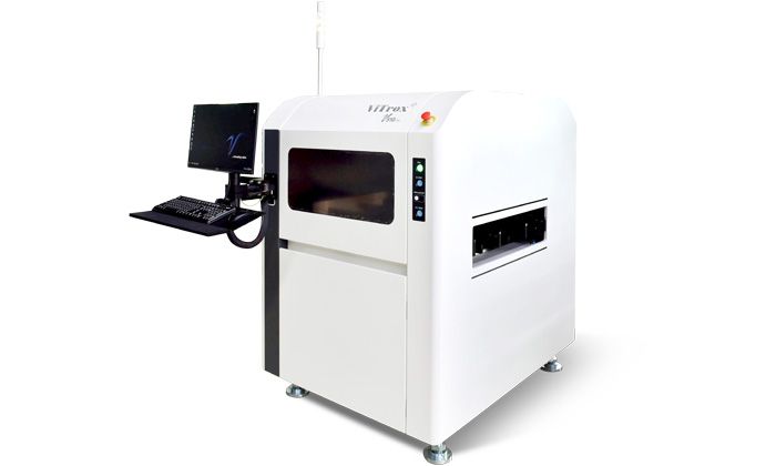 #### Key Benefits: **High-Speed Inspection with Real 3D Measurement:** Achieve rapid and precise inspections, ensuring high-quality output with minimal downtime. **AI-Powered Technology for Smart Programming:** Leverage AI-driven technology for effortless, high-quality programming, minimizing the need for skilled labor while enhancing consistency and accuracy. **Smart Manufacturing Ready:** Fully compatible with Industry 4.0 standards, our AOI system is prepared for the future of smart manufacturing. **Preferred by Leading Contract Manufacturers:** Trusted by the world’s top contract manufacturers for its reliability and performance. **Shareable Spare Parts:** Maximize cost-efficiency with interchangeable spare parts between 3D AOI and 3D API systems, reducing inventory and maintenance costs. **Competitive Cost of Ownership:** Benefit from a cost-effective solution that delivers high returns on investment through superior technology and reduced operational costs. #### Breakthrough Technologies: **AI-Based Smart Programming:** Our intelligent and automated programming system eliminates reliance on human skills, drastically improving programming speed while ensuring IPC class compliance for algorithm and parameter settings. **AI Assist Buy-Off in Repair Station:** The AI Smart Assist feature accelerates the inspection buy-off process, reducing errors and enhancing accuracy, perfectly aligning with smart manufacturing requirements. **Largest Board Size Platform:** Accommodates large PCB boards up to 1.3m x 1.3m and weighing up to 25kg, making it ideal for handling the most demanding inspection tasks. **New Side Camera with SPECKLE Auto Mapping Technology (SAM):** Integrates auto-mapping for component lead inspection from side angles, supporting advanced algorithm-driven inspection and adaptive lighting for precise results. **Unique and Universal Algorithms:** Our AOI system is not just for standard SMT but also addresses unique inspection needs like gold finger inspections, coordinate measurement, and surface defect detection. Our AOI solution delivers world-class inspection capabilities, ensuring quality-assured results and compatibility with Industry 4.0. Its advanced features and breakthrough technologies make it the go-to choice for manufacturers seeking to enhance their PCB assembly processes.
Cleaning Chemistry (Product Cleaning and Tools Cleaning)
### High-Performance Cleaning Chemistry for PCB and Tools Cleaning In today's advanced electronics manufacturing, PCB cleaning is no longer optional—it's essential, especially in high-end applications. Ensuring that your assembled or mounted PCBs are thoroughly cleaned of production residues, environmental contaminants, and handling dirt is crucial for reliable further processing and trouble-free performance. #### Key Features: **Fully Automatic High-End Batch Cleaner:** Our state-of-the-art batch cleaner is designed for precision and efficiency, delivering consistent cleaning results across all your assemblies. **Versatile Capacity:** Capable of handling screens, stencils, carriers, washing frames, PCBAs, misprints, and squeegees up to 770 x 950 mm (31" x 37"), this cleaner is adaptable to a wide range of PCB cleaning needs. **Effective Contaminant Removal:** Our cleaning chemistry excels at removing copper oxides (CuO), aluminum oxides, SMD paste, fluxes, and solder pastes from DCBs, PCBAs, ceramic substrates, aluminum, and non-ferrous metals, ensuring your components are free from residues that could impair performance. Investing in our advanced cleaning chemistry and tools cleaning systems guarantees that your assemblies are prepared for reliable further processing, enhancing their performance and longevity. Trust our solutions to maintain the integrity of your high-end electronics and meet the rigorous demands of modern manufacturing.
Cutting Laser System
### Cutting Laser Systems for PCB Assembly The MicroLine 5000 series is a cutting-edge solution for precision drilling and cutting in PCB assembly. With the ability to drill small holes with diameters as minute as 20 μm into various organic and inorganic substrates, it is ideal for applications such as through-hole drilling, blind vias, large mounting holes, and contour cutting of irregular PCB outlines. 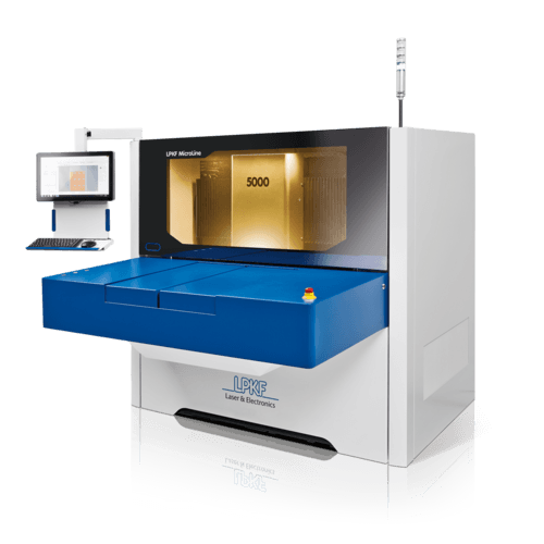 #### Quality and Precision The MicroLine 5000 utilizes a high-quality UV laser that ensures minimal thermal stress zones, even when cutting or drilling sensitive materials. This results in clean edges without dust or burrs. Equipped with powerful laser sources of 10 W, 15 W, and 27 W, the system can be configured to handle different material types and sizes, making it a versatile tool for any PCB assembly line. #### Contour Cutting In addition to its drilling capabilities, the MicroLine 5000 is designed for contour cutting of standard panel sizes up to 533 mm × 610 mm. With a cutting channel width of just 20 μm, this high-quality UV laser can handle even the most demanding contour cuts at high speeds, ensuring both efficiency and precision. #### Advanced Process Monitoring The MicroLine 5000 series is equipped with an integrated vision system that provides fast fiducial recognition for precise alignment. This camera system can utilize virtually any PCB feature as a fiducial mark, enhancing the accuracy of the cutting process. Additionally, an integrated power measurement system ensures reliable and repeatable laser power control at the material level, maintaining consistent quality across all cuts and drills. #### Technical Specifications **Max. Working Area:** 533 mm x 610 mm (21" x 24") **Positioning Accuracy:** +/- 20 µm **Diameter of Focused Laser Beam:** 20 µm **System Dimensions (W x H x D):** 1660 mm x 1720 mm x 1900 mm (66" x 68" x 75") **Weight:** Approx. 2000 kg Height incl. status light = 2200 mm (87") #### Available Variants The MicroLine 5000 series offers two powerful variants: #### MicroLine 5127 **Laser Power:** 27 W **Wavelength:** 355 nm (UV) **Pulse Duration:** Nano second **Series:** 5000 series **CleanCut:** Yes #### PicoLine 5440 **Laser Power:** 40 W **Wavelength:** 355 nm (UV) **Pulse Duration:** Pico second **Series:** 5000 series **CleanCut:** Yes The Cutting Laser Systems are engineered to deliver unmatched precision and quality in PCB manufacturing, making them an essential tool for any production line that demands high accuracy and reliability.
Die Bonding
### Advanced Die Bonding Systems for Precision PCB Assembly Our automatic Die Bonding systems, featuring the Model 6200, offer unmatched versatility in a compact and unique table-top configuration. Designed for precision and efficiency, this system supports a wide range of die attach processes, making it an ideal solution for advanced PCB assembly requirements.  #### Key Features: **Unmatched Versatility:** The Model 6200 allows for the execution of a broad spectrum of die attach processes, including Epoxy Die Attach, various Eutectic processes, GGI using Ultrasonic or Thermo-compression, ACF/ACP, Ag Sintering, Die Stacking, and more. This versatility makes it suitable for diverse applications within a single machine. **High Placement Accuracy:** Achieve exceptional placement accuracy, better than 3 microns (process dependent), thanks to advanced servo systems, a high-resolution digital vision system, and state-of-the-art Windows-based software. This precision ensures reliable and repeatable results in your PCB assembly process. **Wide Component Handling Capability:** The system efficiently handles both active and passive components presented in 2″ and/or 4″ Waffle/Gel packs, various Tape & Reel feeders, and custom Trays. This capability ensures flexibility in component sourcing and handling, enhancing overall productivity. **Compact and Efficient Design:** With its small and unique table-top configuration, the Model 6200 is perfect for environments where space is at a premium while still delivering high-performance die bonding capabilities. **Specification Highlights:** - Work Area up to 170 x 150 mm. - Die size: 0.150 to over 50 mm. - Die Thickness: from 50 µm. - Die Aspect Ratio: over 1:50. - Die Material: GaAs, Silicon, Glass, other. - Die Presentation: - Up to Ten 2” Waffle/Gel packs - Up to 8 Tape & Reel feeders - Volumetric, Time-Pressure, Jet or Other Dispensing. - Single or Double Dispenser. Any combination of the above. - Stamping (pin transfer) for dots as small as 75 µm. - Cold or Hot process up to 500°C with Forming Gas cover. - Heated pickup tool up to 500°C with Forming Gas. - Ultrasonic bonding process available. - Integrated Ag Sintering system. - Integrated UV curing system. - Programmable Bond Line Thickness control. - Advanced Die Stacking capability. - Pickup/Bond Force: 40 – 9000 grams. - Placement Accuracy: better than ±3 µm depending on application. - Throughput: up to 700 CPH depending on application. Our Die Bonding systems are engineered to deliver precision, versatility, and efficiency, making them an essential tool for advanced PCB assembly. Trust in our technology to meet your exacting standards for die attach processes, ensuring high-quality and reliable production outcomes.
Electronic Hand tools
### Electronic Hand Tools for PCB Assembly When it comes to creating or repairing solder joints in PCB assembly, precision and control are paramount. Soldering tools, particularly those operating below 450°C, are essential in ensuring high-quality solder joints, especially in today’s era of sensitive assemblies and components. Temperature-controlled soldering tools are indispensable for both Surface Mount Technology (SMT) and Through Hole Technology (THT), offering optimal soldering results at lower temperatures. 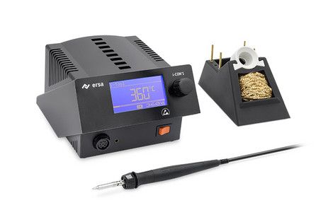 At the forefront of soldering technology, Ersa soldering tools stand out with their reliable functionality, robust and aesthetically pleasing design, and a legacy of industry experience. Whether you're dealing with intricate SMT components or larger THT assemblies, Ersa provides the right soldering and desoldering tool for every application. #### Categories of Hand Soldering Tools **Soldering and Desoldering Stations:** Equipped with temperature-controlled soldering tools, these stations include high-precision soldering irons, THT desoldering tools, SMT tweezers, hot air convection tools, and high-power soldering irons, ensuring precise control and effective soldering in various applications. **Regulated Power Soldering Irons:** Ideal for demanding soldering tasks, these irons offer consistent performance and precision, making them perfect for complex PCB assemblies. **Mobile Soldering Tools:** Designed for flexibility, these tools can be used without a power supply, providing mobility and convenience in on-the-go soldering tasks. **Unregulated Power Soldering Irons:** Best suited for simple or occasional soldering needs, these irons offer a cost-effective solution for less demanding applications. ###### Each tool is designed to meet the specific needs of PCB assembly, ensuring that you have the right equipment for any soldering challenge.
Low-pressure plasma system
### Advanced Low-Pressure Plasma Systems for Versatile PCB Assembly Applications Our Low-Pressure Plasma Systems stand for high-quality and precision, offering solutions that cater to a wide range of plasma processes in PCB assembly. Designed to meet the demands of both production and research and development, our product range includes everything from compact tabletop devices to robust stand-alone systems, each engineered for optimal performance. #### Key Features: **Compact and Versatile:** Our entry-level V6-G tabletop device is ideal for low-pressure plasma applications in batch production and R&D test series, providing a compact yet powerful solution for diverse needs. **Customizable Stand-Alone Systems:** Our stand-alone systems can be customized to suit different plasma-producing frequencies and capacities, making them adaptable for various plasma processes in PCB assembly. **High-Quality Construction:** Every system is built to the highest quality standards, ensuring reliable and consistent performance across all applications. **Flexible Plasma Applications:** These systems are designed for versatility, enabling users to perform a wide range of plasma processes, from surface activation and cleaning to etching and coating, all within a controlled environment. **User-Friendly Design:** With an emphasis on ease of use, our systems feature intuitive controls and robust construction, making them suitable for both seasoned professionals and those new to plasma technology. 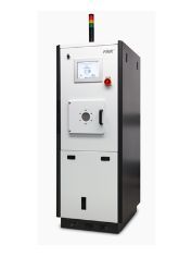 Whether you're working in batch production or conducting R&D, our Low-Pressure Plasma Systems offer the flexibility, precision, and reliability you need to achieve superior results in your PCB assembly processes.
Micro-Material Process
### Advanced Micro Material Process PCBA Solutions for Precision and Versatility Our Micro Material Process PCBA systems are designed to offer unparalleled precision and versatility in PCB assembly, utilizing cutting-edge laser technology to achieve exceptional results. The small focal spot size of the laser beam enables us to produce cut channels with widths as narrow as 15 µm, ensuring precise corner radii and sharp cut edges. This level of accuracy makes our laser systems particularly advantageous for high-frequency (HF) applications where precision is critical. #### Key Features: **Cold Ablation of Thin Films:** Leveraging picosecond lasers, our systems perform cold ablation on various thin films, opening up new possibilities in material processing. The ultrashort pulse width minimizes thermal effects, making it ideal for machining delicate layers used in OLED lighting and complex thin-film solar cells. **Large Bandwidth and Versatile Applications:** Our laser systems offer a broad range of options, making them suitable for a variety of materials and applications. The ability to process different substrates with precision ensures that your PCBA needs are met with the highest standards. **Gentle Machining of Laminated Materials:** Utilizing lasers in the “green” range of the visible light spectrum, our ProtoLaser S4 is optimized for surface machining of PCB materials. This gentle approach is perfect for working with laminated materials such as FR4 boards, ensuring the integrity of the material is maintained. **Precision Machining of Ceramics:** The ProtoLaser U4, equipped with a UV laser source, excels in machining ceramics. It can structure metal layers on ceramic substrates like Al2O3, score ceramics, and is particularly effective for processing Low-Temperature Co-fired Ceramics (LTCCs) through structuring, cutting, and drilling. 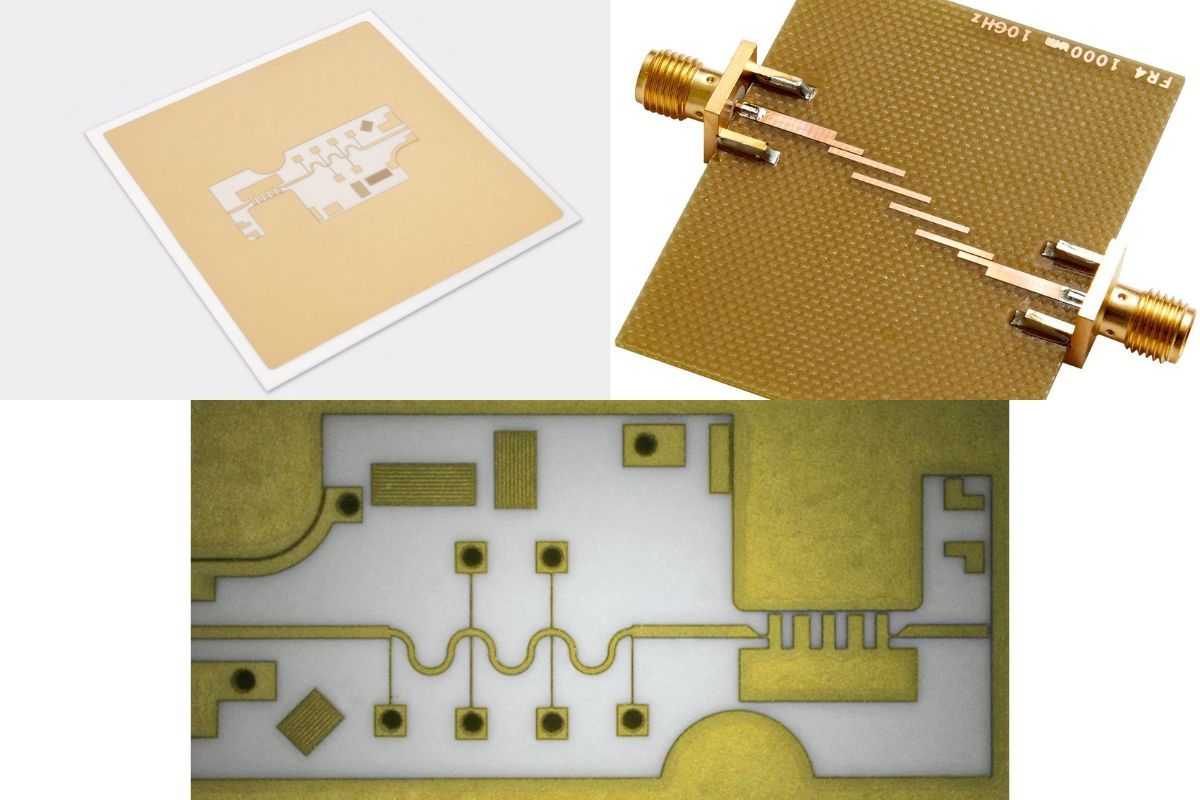 Our Micro Material Process PCBA solutions are at the forefront of PCB assembly technology, delivering precise, reliable, and versatile machining capabilities. Whether you're working with delicate thin films, laminated materials, or ceramics, our systems provide the precision you need to achieve exceptional results.
Reflow Soldering System
### Revolutionizing Reflow Soldering with the Latest Technology Experience a new era in reflow soldering with our cutting-edge systems, designed to deliver unmatched performance, efficiency, and sustainability. Prodrive Technologies from the Netherlands is enhancing its production capabilities with the state-of-the-art Ersa HOTFLOW THREE reflow soldering system, setting a new benchmark in the industry.  #### Key Features: **Superior Uptime and Efficiency:** Achieve inspiring machine uptimes with the 3-stage Ersa SMART CLEANING system, known for its exceptional accessibility and minimal maintenance requirements. Maximize your Overall Equipment Effectiveness (OEE) and throughput with advanced technology. **Rapid Cooling and Profile Change:** Benefit from fast cooling and profile changes with the innovative SMART CONVECTION POWER UNIT (SCPU®), which ensures unparalleled soldering quality and precise control over the soldering process. **Enhanced Performance with Reduced Energy Consumption:** Our reflow soldering systems are engineered for high performance while significantly reducing energy consumption. This not only enhances productivity but also supports sustainable manufacturing practices. **User-Friendly Interface and Software:** Enjoy maximum user-friendliness with an industrial PC featuring a touch screen, making operation intuitive and seamless. Our excellent software provides accurate process data acquisition and easy integration with MES systems through standard interfaces. **Real-Time Data and Traceability:** Ensure full traceability of your soldering process with real-time data standardization. Access critical process information effortlessly, ensuring quality control and compliance at every stage of production.
Robotic Soldering
### Enhance PCB Assembly Efficiency with Advanced Robotic Soldering Solutions Our cutting-edge robotic soldering systems are designed to produce high-quality solder joints with unmatched consistency and precision. Ideal for a range of PCB assembly applications, our soldering robots offer superior performance, enabling fast and efficient soldering processes that maintain stable temperatures, even with fine soldering tips as small as 0.4 mm. #### Key Features: **High Precision and Reliability:** Our soldering robots deliver the highest precision and reliability, ensuring excellent solder joint quality with each application. The precise solder wire feeding system enhances accuracy and consistency, vital for intricate PCB assemblies. **Efficient Production:** Increase your productivity with our double drawer system, which supports continuous production, minimizing downtime and maximizing throughput. **Cost-Effective:** Achieve significant cost savings compared to traditional hand soldering, as our robotic systems reduce labor costs and improve efficiency. **User-Friendly Programming:** Our soldering robots feature simple and intuitive programming, making it easy for operators to set up and manage the soldering process with minimal training. **Complete Process Traceability:** Ensure complete traceability of the soldering process, with comprehensive data tracking that supports quality control and compliance with industry standards. Our robotic soldering solutions are designed to meet the demanding requirements of modern PCB assembly, delivering high-quality results while reducing costs and enhancing productivity. Trust in our technology to take your soldering processes to the next level.
SMD,BGA,PTH Rework System
### Award-Winning SMT and BGA Rework Systems When it comes to the repair of electronic assemblies, Ersa Rework Systems stand out with their cutting-edge Infrared (IR) and Hybrid Rework technology. Renowned for their exceptional price/performance ratios and patented innovations, these systems have earned their place at the forefront of the market. Even in the most demanding SMT and BGA rework applications, Ersa Rework Systems deliver repeatable, best-in-class results from the very first process.  #### Key Technical Highlights: **High-Precision Axis System:** The X, Y, Z axis system combined with high-resolution cameras ensures precise component placement. **Automated Processes:** Features automated component placement, soldering, and desoldering for consistent and reliable performance. **Hybrid Heating Head:** Incorporates two heating zones for controlled and efficient heating. **Powerful IR Underheating:** Large-area infrared underheating is segmented into three zones, ensuring even heat distribution. **Non-Contact Temperature Measurement:** Equipped with a digital sensor for accurate, real-time temperature monitoring. **Accu-TC Sensor Integration:** Three K-type thermocouple inputs for enhanced temperature accuracy and process control. **Effective Cooling:** The system utilizes compressed air for effective assembly cooling, preventing overheating and ensuring process stability. **Gentle Heating Technology:** Ensures safe and effective heating without damaging sensitive components. **Sensor-Guided Soldering Processes:** Provides precise control and repeatability in soldering operations. **Contactless Residual Solder Removal:** Enhances the quality of rework by removing residual solder without physical contact. **Complete Process Documentation:** Offers clear user guidance and comprehensive documentation for traceability and process improvement. **Process Observation:** Monitored with up to 8 thermocouples for precise process control. **Machine Vision:** Ensures accurate component alignment and placement. **User-Independent Results:** Ensures reproducible repair results through automated processes. **Dip & Print Station Compatibility:** Facilitates seamless integration with additional rework stations. Elevate your rework capabilities with Ersa's industry-leading technology, designed to meet the challenges of modern SMT and BGA applications. Learn more about how Ersa Rework Systems can enhance your electronic assembly processes.
SMT Pick and Place Machines
### Maximize Productivity with Our Pick & Place Systems for PCB Assembly Our advanced Pick & Place Systems are designed to optimize your PCB assembly process, offering unparalleled flexibility, speed, and precision. Whether you're focused on high-volume production or prototyping, our diverse range of surface mount line solutions ensures you can meet your production goals while minimizing downtime. #### Key Features: **Flexible Machines:** Adapt to varying production demands with our flexible Pick & Place machines, capable of handling a wide range of PCB assembly requirements. High-Speed Performance: Achieve rapid assembly with our high-speed machines, offering speeds ranging from 15,000 to 104,000 components per hour, ensuring your production line runs efficiently. **High Feeder Capacity:** Benefit from our feeder capacity supporting up to 264 positions x 8mm, allowing for efficient handling of multiple components and maximizing production throughput. **Prototyping Options:** Perfect for both large-scale production and small-batch prototyping, our systems provide the versatility needed for various stages of product development. **Multiple Head Configurations:** Choose from 1-head to 4-head configurations to match your specific production needs, enabling you to balance speed and precision. **Wide Range of Feeders:** Accommodate a variety of component types and sizes with our extensive range of feeders, ensuring smooth and uninterrupted production. Our Pick & Place Systems are engineered to deliver superior performance, enhancing your productivity and reducing operational downtime. Trust our cutting-edge technology to keep your PCB assembly line running at peak efficiency.
Selective Soldering System
### Advanced Selective Soldering Systems for Precision PCB Assembly Our Selective Soldering systems are engineered to deliver exceptional precision and efficiency in PCB assembly, accommodating a wide range of board sizes and configurations. Whether you're working with small-scale prototypes or high-volume production, our systems are designed to meet the diverse demands of modern electronics manufacturing.  #### Key Features: #### Versatile Dimensions: **VERSAFLOW 4 XL:** Length: 4,700 mm, Width: 1,800 mm, Height: 1,600 mm. Supports PCB widths from 50 mm to 610 mm, lengths from 127 mm to 508 mm (optional up to 1,200 mm), and weights up to 20 kg. **VERSAFLOW 3/66 XL:** Length: 10,150 mm, Width: 1,900 mm, Height: 1,650 mm. Capable of handling PCBs with widths from 100 mm to 610 mm and lengths up to 3,000 mm, with a maximum weight of 20 kg. **ECOSELECT 4:** Length: 2,000 mm, Width: 1,800 mm, Height: 1,700 mm. Ideal for PCB widths from 50 mm to 508 mm, lengths from 127 mm to 508 mm, and weights up to 15 kg. **POWERFLUX:** Compact with a length of 1,689 mm, width of approx. 1,080 mm, and height of approx. 1,557 mm, supporting PCBs up to 508 mm in both width and length, and a maximum weight of 8 kg. **Flexible Conveyor Support:** Options include roller conveyors and chain pin conveyors, accommodating a range of PCB sizes and ensuring smooth transport throughout the soldering process. #### Flux / Preheat / Solder Modules: **Fluxer:** Drop-Jet and VERSAFLUX modules, offering precision spray flux systems with up to 2 spray heads per axis for accurate flux application. **Preheater:** Available with IR heating, convection, or a combination of both, ensuring optimal preheating of the PCB for reliable soldering results. **Soldering Module:** Equipped with electromagnetic solder pots and mini-wave soldering options, capable of handling up to 6 pots with a solder volume of 13 kg per pot, providing flexibility for various soldering tasks. **High Capacity and Precision:** Our systems are designed to handle maximum PCB clearances of up to 120 mm on the top side and 60 mm on the bottom side, ensuring compatibility with a wide range of PCB designs. **Efficiency and Performance:** With dimensions tailored for different production needs, from compact setups to large-scale operations, our selective soldering systems are built on robust foundations to ensure long-term reliability and performance. Enhance your PCB assembly line with our state-of-the-art Selective Soldering systems, designed to deliver unmatched precision, flexibility, and efficiency. Explore the perfect solution for your soldering needs and experience the difference in quality and performance.
Solder Paste Printer
### Precision and Efficiency with Advanced Solder Paste Printer Technology Our cutting-edge Solder Paste Printer utilizes the latest in measurement technology with the 3D LIST camera, ensuring the highest accuracy in solder paste application. This innovative technology is crucial for producing consistent solder paste depots, which directly influence the printed volume and the final quality of the solder joint. #### Key Features: **3D LIST Camera Technology:** The 3D LIST camera precisely measures the shape and height of the smallest solder paste depots, ensuring uniformity across the entire surface. This advanced technology helps prevent issues like sloping edges, which can compromise the quality of the solder joint. **ULTRA³ Integration:** Our ULTRA³ system combines a stencil printer and 3D-SPI (Solder Paste Inspection) in one, providing real-time quality control during the printing process. This integrated approach ensures that any deviations in paste deposits are immediately detected and corrected. **Substrate Handling and Parallel Processing:** Designed for efficiency, the printer allows for simultaneous substrate handling and parallel processing, reducing downtime and increasing throughput. **Intelligent Stencil Cleaning:** Equipped with an intelligent stencil cleaning system, the printer offers customizable cleaning modes, including wet, dry, and vacuum cleaning. This ensures that the stencil remains clean and effective throughout the production process. **Controlled Paper Feed:** The controlled paper feed system allows for reproducible cleaning cycles, optimizing material consumption and maintaining consistent cleaning performance. **Advanced Printhead and Squeegee Design:** The printer features a state-of-the-art printhead and squeegee system, delivering precise control over the solder paste application process, ensuring consistent results across each production run.  Our Solder Paste Printer is designed to deliver unmatched precision and efficiency, ensuring that every component in your PCB assembly meets the highest standards of quality. Experience superior performance with our innovative solder paste printing technology.
Storage for ESD material
### Optimize Your PCB Manufacturing with Precise SMT Temperature and Humidity Control In the intricate world of PCB manufacturing, maintaining strict control over temperature and humidity is crucial. The right environmental conditions on the manufacturing floor can make all the difference between producing flawless PCBs and encountering costly defects. This article delves into the significance of temperature and relative humidity (Rh) control in PCB assembly and offers insights into achieving precision in your operations.  The F1 dry cabinet is a cutting-edge solution designed to maintain an internal humidity level as low as 1% RH. This makes it the ideal choice for moisture-proof and anti-oxidation storage applications. Whether you're storing precision metal parts, miniature devices, pharmaceutical substances, biotic specimens, batteries, crystals, IC package modules, optical lenses, MSD, MBB, or scientific precision instruments, the F1 dry cabinet offers unparalleled protection against corrosion, mold, and deterioration. iX2B is specially designed for moisture sensitive devices of level 4,5,5A,or 6. The iX2B can eliminate oxidation of stored parts. So it is useful for storing parts such as precision metal parts, miniature devices, pharmaceutical substance, biotic specimens, battery, crystal, IC package module, optical lens or scientific precision instruments..etc. 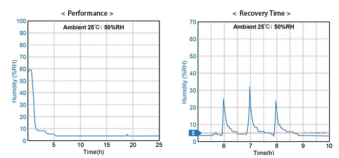 Additionally, our customized dry box services cater to specific storage needs, including Tape Feeder Cabinets and Tape Reel Storage Cabinets, ensuring that every component of your PCB assembly process is stored under optimal conditions. Ensure the longevity and reliability of your sensitive materials with our state-of-the-art storage solutions, designed to meet the rigorous demands of modern PCB manufacturing.
Vacuum-soldering
### Advanced Vacuum Soldering Systems for Void-Free Soldering Achieve high-quality solder connections with our cutting-edge vacuum soldering systems, specifically designed to meet the demanding requirements of modern electronic components such as power modules, hybrid, and multichip components. As the power density of these components continues to rise, ensuring the reliability and performance of solder connections has never been more critical. #### Key Features of Our Vacuum Soldering Systems: Void-Free Solder Connections: Our vacuum soldering technology systematically eliminates gas inclusions (voids) from the liquid solder, ensuring perfect, void-free solder joints essential for high-performance applications. **High-Quality Production:** Engineered for excellence, our systems deliver superior soldering results, even for large power modules, using preform solders and solder pastes in a continuous, controlled process. **Optimized for Advanced Components:** Designed to handle the increasing power density of advanced electronic components, our vacuum soldering solutions meet the rigorous quality demands of today’s electronics manufacturing. **Intelligent Temperature Management:** Benefit from short cycle times and high throughput thanks to our advanced temperature management system, which ensures consistent and efficient soldering performance. **Environmentally Friendly Design:** Our vacuum soldering systems are not only powerful but also environment-friendly, featuring a smart design that is easy to operate and maintain. **Flexible Soldering Technologies:** We offer customizable soldering solutions tailored to meet individual customer requirements, ensuring that our systems align with your specific production needs. **Reproducible Results:** Our continuous process control guarantees perfect and reproducible soldering results, making our systems the ideal choice for high-reliability applications. With our vacuum soldering systems, you can achieve unparalleled soldering quality and reliability, ensuring that your electronic components meet the highest standards of performance and durability.
Wave Soldering
### Ersa POWERFLOW Wave Soldering Systems for High-Performance PCB Assembly Ersa POWERFLOW wave soldering systems are engineered to meet diverse customer requirements, ranging from high-end full-tunnel inert gas soldering systems to open atmospheric wave soldering systems. Designed for modern wave soldering applications with formats up to 610 × 850 mm, these systems offer stable processes and reproducible parameters, ensuring exceptional availability, economy, and quality. 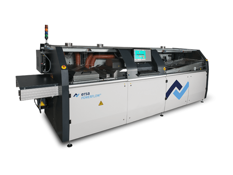 #### Key Features: **Versatile Soldering Solutions:** Tailor your wave soldering process with systems that adapt to both high-end inert gas soldering and open atmospheric wave soldering, providing flexibility for a wide range of applications. **Stable and Reproducible Processes:** Rely on consistent, stable processes and parameters that deliver reliable results, making it easy to master any wave soldering task efficiently and effectively. **Powerful Performance:** Benefit from a powerful wave soldering system that offers an impressive price/performance ratio, ensuring cost-effective production without compromising on quality. **Modular and Flexible Preheating:** Customize your preheating process with a modular and flexible preheating concept that can be configured variably in terms of length and output, and can even be retrofitted to meet evolving needs. **Comprehensive Monitoring and Documentation:** Keep track of all process-relevant data with advanced monitoring and documentation capabilities, ensuring your wave soldering process is always ready for traceability. Ersa POWERFLOW wave soldering systems provide the flexibility, power, and reliability needed to excel in modern PCB assembly. With the ability to configure and expand based on specific requirements, these systems are the ideal choice for achieving high-quality wave soldering results in a cost-effective manner.
Wire Bonding
### Wire Bonding Solutions for R&D and Small-Scale Production Our advanced Wire Bonders are specifically engineered for multi-purpose applications in research and development, as well as small series production. These semi-automatic tools are designed with a focus on robustness, reliability, and ease of use, ensuring they meet the diverse needs of your PCB assembly processes. 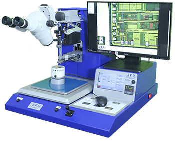 #### Key Features of Our Wire Bonding Equipment **Versatile Bonding Capabilities:** Our equipment supports various bonding techniques, including wedge bonding, ball bonding, and bump bonding. Whether working with aluminum, gold, or ribbon wires, our bonders deliver precise and consistent results. #### WB100e Manual & Semi-Automatic Wire Bonder: - Equipped with a motorized Z-axis for enhanced control and precision. - Large bonding height capability to accommodate various components. - Offers full manual Z bonding for flexible application needs. - Includes an XY manipulator for easy and accurate positioning. #### WB200e Manual & Semi-Automatic Wire Bonder: - Features vibration-free operation for superior bond quality. - Programmable X & Y bond locations ensure precise and repeatable results. - Integrated motorized Z-axis for advanced control during bonding. - Large bonding height capability for handling a wide range of applications. - Offers full manual Z bonding with additional features such as Auto-Bond mode for precision bonding. - Loop control and a vertical camera with crosshair for exact placement and monitoring. Our wire bonders are not only built for durability but also for flexibility, making them ideal for a variety of applications. Whether you are conducting R&D or managing small-scale production, these tools are designed to meet your exact needs with precision and ease.
X-Ray and CT Inspection
### PCB 3D X-Ray Inspection System Elevate your PCB assembly quality with our advanced PCB 3D X-Ray Inspection System, designed to enhance production efficiency and drive cost savings across various sectors, including Electronic Manufacturing Services (EMS), Original Equipment Manufacturers (OEMs), and Original Design Manufacturers (ODMs). Our state-of-the-art system is engineered to meet the diverse needs of modern electronics manufacturing with precision and speed. 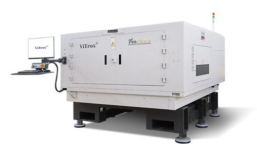 #### Key Benefits **High-Speed Inspection:** Experience rapid inspection capabilities that accelerate your production line and ensure timely quality control. **Powerful Test Algorithms:** Our robust algorithms cover a comprehensive range of market test components, delivering thorough and accurate results. **Lightning Fast Programming:** Streamline your setup with our intuitive programming interface, designed for smart and efficient operation. **Versatile Platform:** Accommodates various board sizes with flexibility, ensuring compatibility with a broad spectrum of PCB assemblies. **World-Leading AXI Solution:** Benefit from the leading Automated X-Ray Inspection (AXI) technology, recognized for its exceptional performance and reliability. **Global Support:** Enjoy unparalleled support with our worldwide coverage, ensuring assistance whenever and wherever you need it. ### Breakthrough Technologies **Lightning Programming:** Simplify your programming process with our Offline Programming (OLP) software. Develop and test programs on your PC without direct machine connection. The drag-and-drop interface facilitates easy programming, while the inline OLP concept minimizes system downtime, boosting overall product throughput. **Largest Board Size Platform:** Accommodate large and heavy PCB boards with our system's impressive capabilities. It handles panel sizes from 127mm x 127mm to 1320.8mm x 1320.8mm, thicknesses from 1.5mm to 10mm, and weights up to 25kg, making it ideal for extensive and demanding applications. **Algebraic Reconstruction Technique (ART):** Our innovative CT technology provides alternative 3D views of defects, enhancing confidence in defect assessment and offering comprehensive failure analysis for ongoing improvements. **Backdrill Inspection:** Improve signal integrity with our advanced backdrilling technique. By removing unused stubs or copper barrels from through-holes, our system reduces signal degradation and via-to-via crosstalk, ensuring optimal performance for high-speed multi-layered boards. Upgrade your PCB assembly inspection with our cutting-edge 3D X-Ray Inspection System and experience unmatched precision, efficiency, and support. Contact us today to learn more about how we can enhance your production processes and quality assurance.


Interested in PCB Assembly Equipment?
Talk to our specialists for a customised solution.
Request a Quote